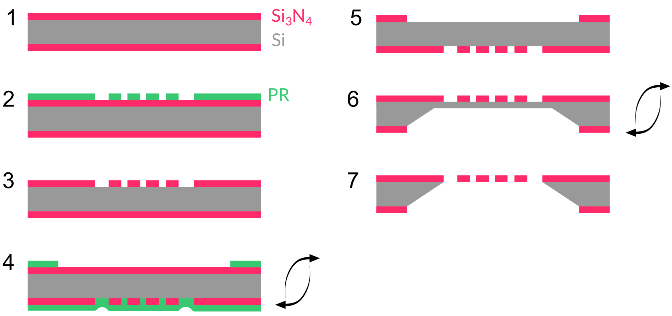
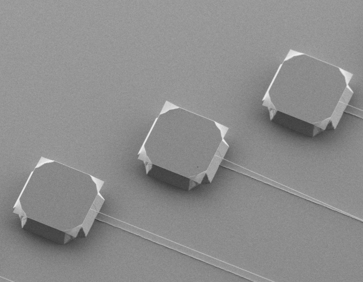
A fabrication method for large-area, high-stress LPCVD \mathrm{Si_3N_4} membranes is presented. These devices can be used as mechanical resonators with very low dissipation, exploiting dissipation dilution. A phononic crystal pattern allows to work with a high-order localized mode, shielded from acoustic radiation in the substrate. The procedure is amenable to most research clean rooms, requiring conventional lithography techniques and wet etching in KOH for device undercut.
Results (3)
We describe the fabrication of high-stress Si_3N_4 nanobeam resonators with high aspect ratios exceeding lengths of 3.5mm. The lowest order out-of-plane modes of these nanobeams have quality factors of Q\geq 10^6 with fundamental mode frequencies lying in the range of 80-500kHz. The beams are fabricated from high-stress, 20-50nm-thick films of Si_3N_4 deposited via LPCVD on standard silicon wafers. The beams are patterned via electron beam lithography and deep reactive ion etching. The underlying silicon is ...
Alumina (\mathrm{Al_2O_3}) films are widely used in photonics and superconducting circuits as an etch stop or passivation layer. In silicon nitride (\mathrm{Si_3N_4}) fabrication, a widely used etching recipe is dry etching using a mixture of \mathrm{SF_6/CHF_3} gasses. In case of multi-stacked materials, one might be interested to etch the \mathrm{Si_3N_4} layer with an stop layer to protect the rest of the stack from the etching step. \mathrm{Al_2O_3} is a great etch stop layer for \mathrm{Si_3N_4} ...
Results per page