Search

Tooltip
Photo by Mohammad Bereyhi, EPFL - LPQM

Results (5)


Electron beam lithography and pattern transfer on membrane grids for transmission electron microscopy

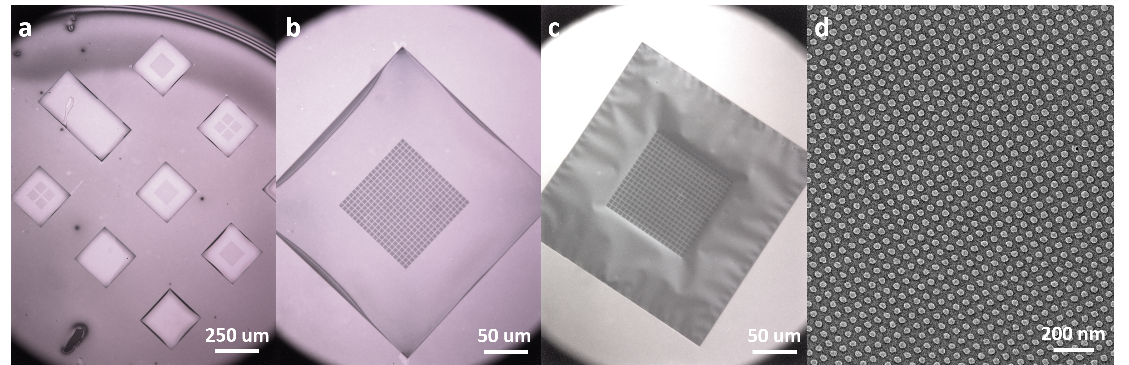
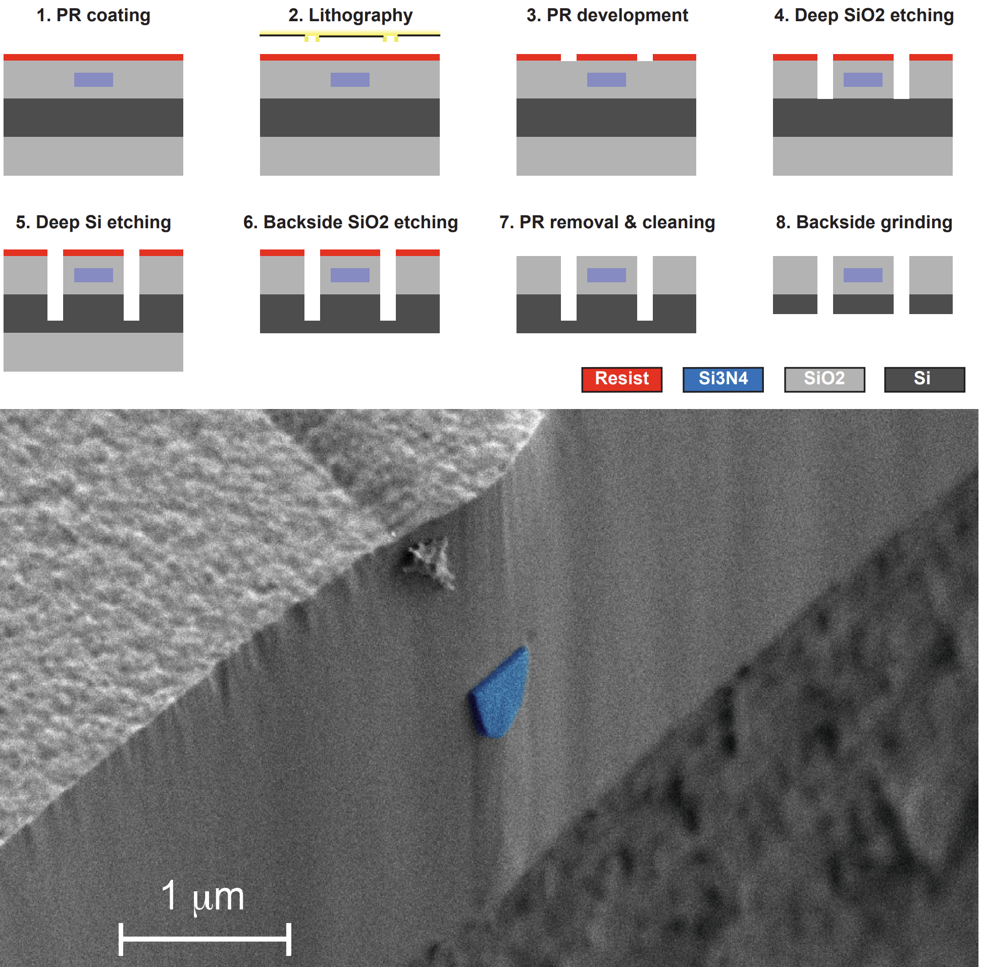
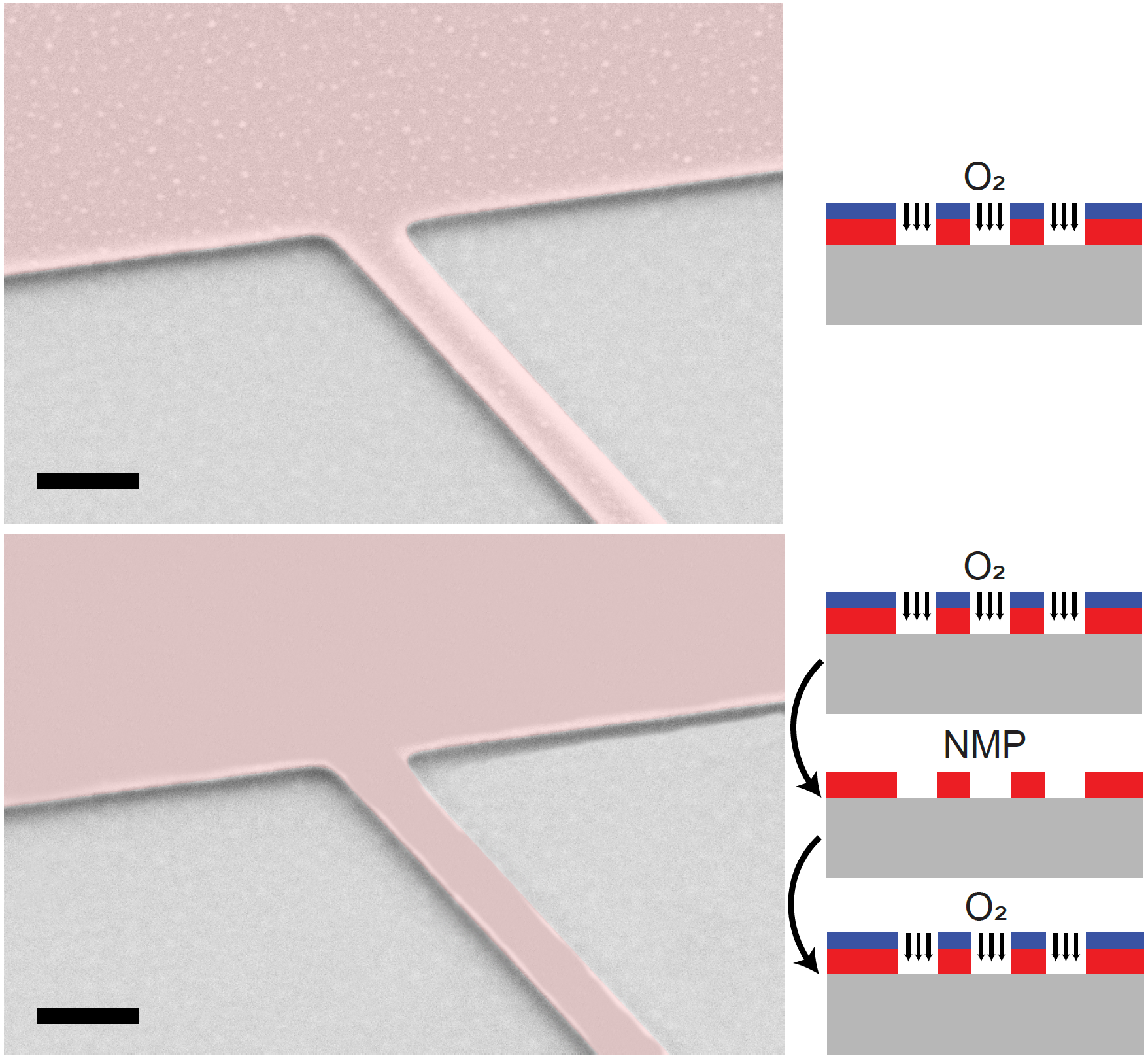
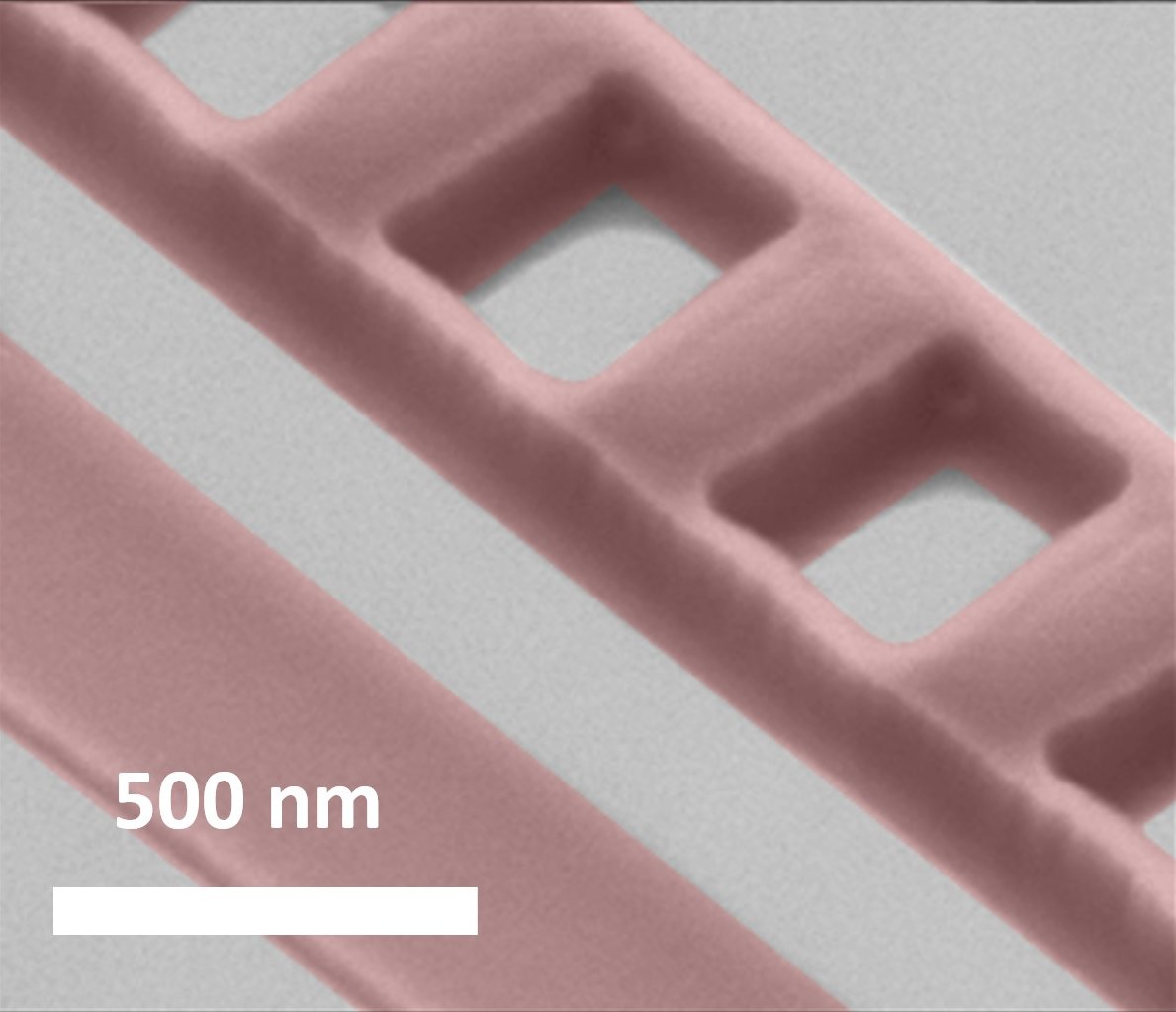
We describe a fabrication process for electron beam lithography (EBL) and the following pattern transfer steps on transmission electron microscope (TEM) grids. For demonstration purposes, we use commercial off-the-shelf TEM grids consisting of a thin suspended silicon nitride membrane on a silicon frame supporting substrate. For the pattern transfer, we demonstrate both an additive patterning technique with metal deposition and lift-off, and a subtractive patterning technique with reactive ion etching. This process could enable direct ...

Version
Version 1.1
Date
2 years, 6 months ago
Lab
EPFL - LPQM
Comments
0
Viewed
1700
Downloads
535
Liked
3


Efficient removal of ZEP ebeam resist after dry etching

Resist removal is an essential step for multi-layer lithography processes where a clean and contamination-free surface is essential to avoid shadow etching patterns from resist leftovers. We show that a short \mathrm{O_2} plasma exposure followed by a full NMP solution cycle removes the resist fully and leaves the surface contamination free.

Version
Version 1.0
Date
2 years, 9 months ago
Lab
EPFL - LPQM
Comments
0
Viewed
2138
Downloads
789
Liked
3

Bulk and Sleeve Electron Beam Lithography for Silicon Nitride Photonic Crystals

This is a method to improve the quality of lithography - in particular electron beam lithography (EBL). During an EBL exposure the electrons undergo different scattering processes. One scattering process that plays an important role is the back scattering of the electrons from the substrate or different stacks of thin film present in the exposure stack. As a result the actual dose that the resist sees is quite different that the original exposure dose. This ...

Version
Version 1.0
Date
3 years, 10 months ago
Lab
EPFL - LPQM
Comments
0
Viewed
2172
Downloads
1109
Liked
1

Fabrication of high-aspect ratio Si_3N_4 nanobeam resonators

We describe the fabrication of high-stress Si_3N_4 nanobeam resonators with high aspect ratios exceeding lengths of 3.5mm. The lowest order out-of-plane modes of these nanobeams have quality factors of Q\geq 10^6 with fundamental mode frequencies lying in the range of 80-500kHz. The beams are fabricated from high-stress, 20-50nm-thick films of Si_3N_4 deposited via LPCVD on standard silicon wafers. The beams are patterned via electron beam lithography and deep reactive ion etching. The underlying silicon is ...

Version
Version 1.0
Date
3 years, 10 months ago
Lab
EPFL - LPQM
Comments
2
Viewed
1550
Downloads
720
Liked
2