We describe a fabrication process for electron beam lithography (EBL) and the following pattern transfer steps on transmission electron microscope (TEM) grids. For demonstration purposes, we use commercial off-the-shelf TEM grids consisting of a thin suspended silicon nitride membrane on a silicon frame supporting substrate. For the pattern transfer, we demonstrate both an additive patterning technique with metal deposition and lift-off, and a subtractive patterning technique with reactive ion etching. This process could enable direct ...
Results (5)
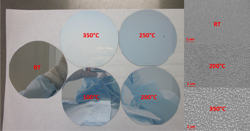
Here we present our study of the stress dependence in Al thin films on deposition conditions. We consider two types of Al 100-nm thick films: E-beam evaporated films and films obtained by magnetron sputtering. We investigate the Al film stress hysteresis in the environment with slowly increasing and decreasing temperature, i.e. during the gradual annealing. We consider the effect of deposition temperature on the film stress and grain size. We conclude that the annealing of ...
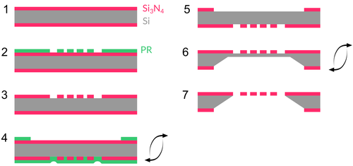
A fabrication method for large-area, high-stress LPCVD \mathrm{Si_3N_4} membranes is presented. These devices can be used as mechanical resonators with very low dissipation, exploiting dissipation dilution. A phononic crystal pattern allows to work with a high-order localized mode, shielded from acoustic radiation in the substrate. The procedure is amenable to most research clean rooms, requiring conventional lithography techniques and wet etching in KOH for device undercut.
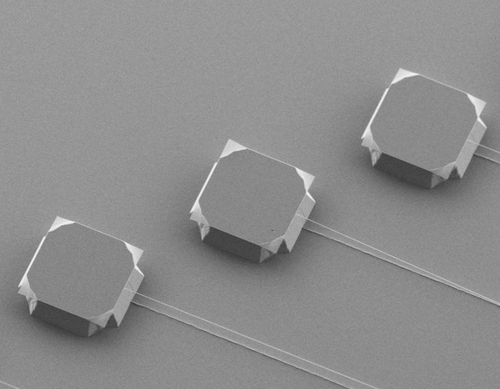
We describe the fabrication of high-stress Si_3N_4 nanobeam resonators with high aspect ratios exceeding lengths of 3.5mm. The lowest order out-of-plane modes of these nanobeams have quality factors of Q\geq 10^6 with fundamental mode frequencies lying in the range of 80-500kHz. The beams are fabricated from high-stress, 20-50nm-thick films of Si_3N_4 deposited via LPCVD on standard silicon wafers. The beams are patterned via electron beam lithography and deep reactive ion etching. The underlying silicon is ...
Releasing mechanical structures is a fundamental step in MEMS processing. Given the wide usage of silicon nitride ( \mathrm{Si_3N_4} ) on silicon (Si) carrier due to high stress and high mechanical Q factors, high etching selectivity between \mathrm{Si_3N_4} and Si is very crucial for the release process. Here we demonstrate that UV light from ambient light sources in a cleanroom environment (EPFL - CMi) can increase the etch rate of \mathrm{Si_3N_4} ...
Results per page


