Electron beam lithography and pattern transfer on membrane grids for transmission electron microscopy

Abstract
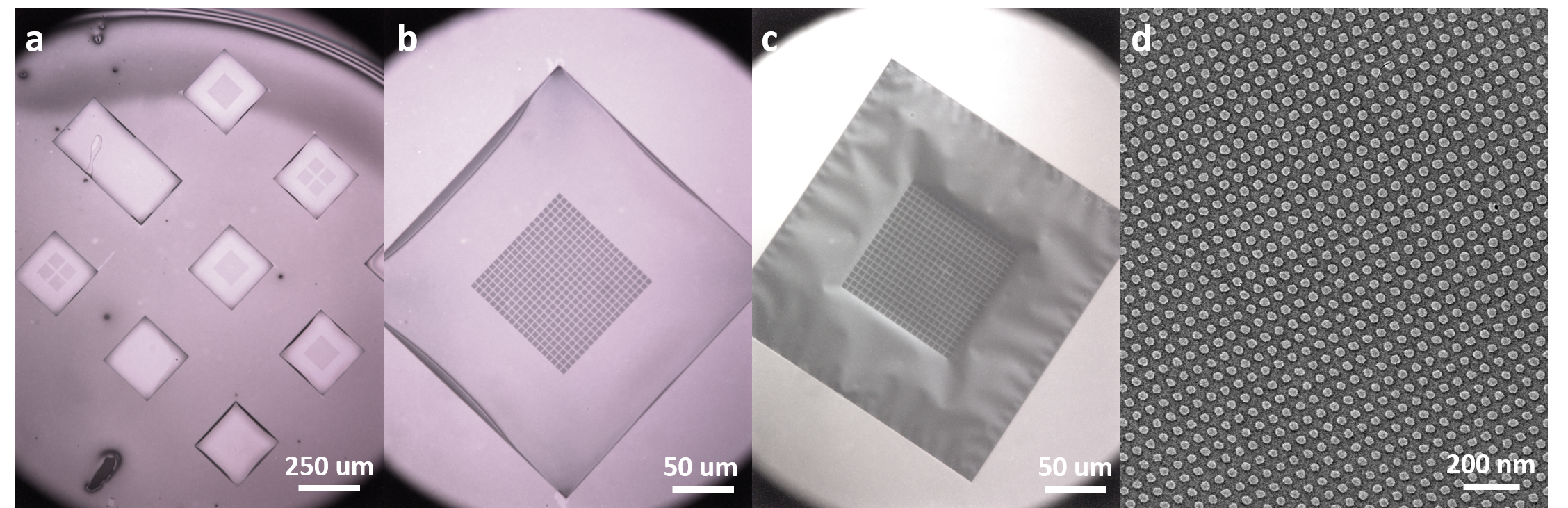
We describe a fabrication process for electron beam lithography (EBL) and the following pattern transfer steps on transmission electron microscope (TEM) grids. For demonstration purposes, we use commercial off-the-shelf TEM grids consisting of a thin suspended silicon nitride membrane on a silicon frame supporting substrate. For the pattern transfer, we demonstrate both an additive patterning technique with metal deposition and lift-off, and a subtractive patterning technique with reactive ion etching. This process could enable direct nanofabrication on TEM grids for electron microscopy and spectroscopy, optical elements for electron and charged particle beams, as well as suspended or membrane-based nanoscale devices.

References
[1] R. G. Hobbs, V. R. Manfrinato, Y. Yang, S. A. Goodman, L. Zhang, E. A. Stach, and K. K. Berggren, Nano Letters 16, 4149 (2016), publisher: American Chemical Society. [2] Y. Yang, C.-S. Kim, R. G. Hobbs, P. D. Keathley, and K. K. Berggren, Ultramicroscopy 217, 113053 (2020).

Share

Authors
-
 EPFL - LPQM


Citations

 Waiting for citation...

Statistics


Comments (0)
Log in to comment & reply