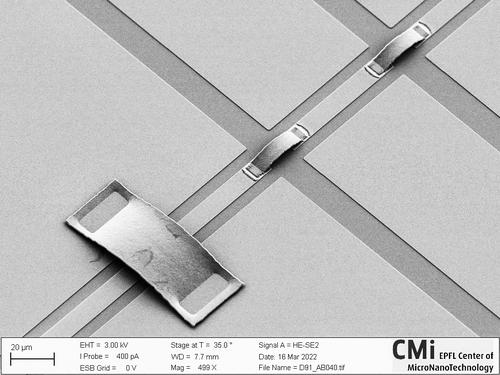
Here we discuss the wafer-scale fabrication process flow of aluminium airbridges for microwave (MW) interconnects on lithium niobate on Damascene silicon nitride (LNOD) photonic chips. We also discuss the subsequent chip release procedure that preserves the bridges allowing for safe release of these delicate structures.
Results (5)
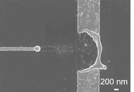
We highlight some stability issues in high-surface-area and high-aspect ratio gold nanostructures fabricated using inorganic adhesion layers on silica substrates. We ascribe these problems to capillary and surface effects and show the use of organic silane self-assembled monolayers to improve the long-term stability of such structures.
We describe a fabrication process for electron beam lithography (EBL) and the following pattern transfer steps on transmission electron microscope (TEM) grids. For demonstration purposes, we use commercial off-the-shelf TEM grids consisting of a thin suspended silicon nitride membrane on a silicon frame supporting substrate. For the pattern transfer, we demonstrate both an additive patterning technique with metal deposition and lift-off, and a subtractive patterning technique with reactive ion etching. This process could enable direct ...
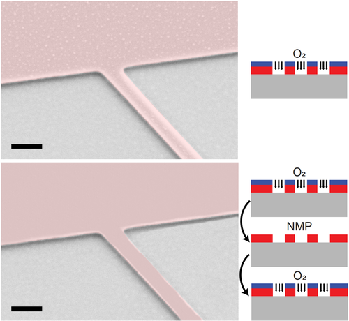
Resist removal is an essential step for multi-layer lithography processes where a clean and contamination-free surface is essential to avoid shadow etching patterns from resist leftovers. We show that a short \mathrm{O_2} plasma exposure followed by a full NMP solution cycle removes the resist fully and leaves the surface contamination free.
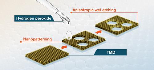
Here we will discuss our novel anisotropic wet-etching method that allows scalable fabrication of TMD metamaterials with atomic precision, combined with traditional nanolithography techniques.[1] We show that TMDs can be etched along certain crystallographic axes, such that the obtained edges are atomically sharp and exclusively zigzag-terminated. This allows us to fabricate interesting hexagonal nanostructures of predefined order and complexity, including a few nanometer thin nanoribbons and nanojunctions.
Results per page


