Abstract
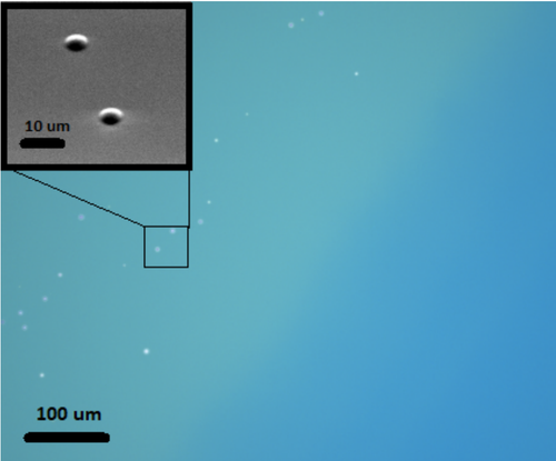
Alumina (\mathrm{Al_2O_3}) films are widely used in photonics and superconducting circuits as an etch stop or passivation layer. In silicon nitride (\mathrm{Si_3N_4}) fabrication, a widely used etching recipe is dry etching using a mixture of \mathrm{SF_6/CHF_3} gasses. In case of multi-stacked materials, one might be interested to etch the \mathrm{Si_3N_4} layer with an stop layer to protect the rest of the stack from the etching step. \mathrm{Al_2O_3} is a great etch stop layer for \mathrm{Si_3N_4} etching. Here, we look at the selectivity of the etching process between \mathrm{Si_3N_4} and \mathrm{Al_2O_3} available at EPFL cleanrooms (CMi) using the SPTS dry etching tool. In addition we observe formation of pinholes in the \mathrm{Al_2O_3} film after deposition of LPCVD \mathrm{Si_3N_4} layer. We attribute the pinholes to formation of aluminium oxinitride compounds (\mathrm{Al_xO_yN_z}). The effect is reduced in lower alumina thickness, but still present. This is a limitation in using alumina as an etch stop for silicon nitride dry etching.

References
[1] Bermudez, V. M. "Observation of adsorption and reaction of NH 3 on crystalline Al 2 O 3 under steady-state conditions using external-reflection infrared spectroscopy." Journal of Vacuum Science & Technology A: Vacuum, Surfaces, and Films 16.4 (1998): 2572-2580.

Citations

 Waiting for citation...


Statistics


Links


Comments (0)
Log in to comment & reply