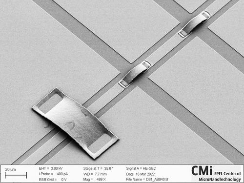
Here we discuss the wafer-scale fabrication process flow of aluminium airbridges for microwave (MW) interconnects on lithium niobate on Damascene silicon nitride (LNOD) photonic chips. We also discuss the subsequent chip release procedure that preserves the bridges allowing for safe release of these delicate structures.
Results (5)
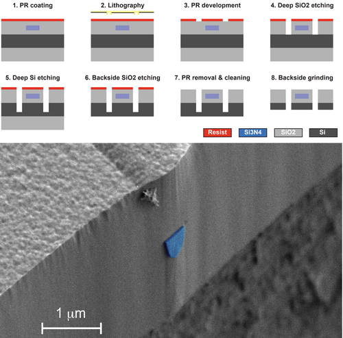
This short article describes a method to separate a wafer into photonic chips or dice, using dry etching and backside grinding. This method enables smooth chip facets that are advantageous for edge coupling with fibers or other chips.
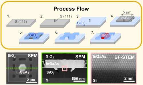
This work was presented at the Nanofabrication Photonics Online Meetup, 16-18 May 2021. Template-assisted selective epitaxy enables the local integration of group III-V semiconductors on Si with high material quality for nanophotonic applications. Here we demonstrate evidence of room temperature lasing at 1530 nm for a monolithically integrated InGaAs whispering gallery mode cavity on Si with a thickness of 300 nm and a diameter of 1.5 µm. These devices can potentially be scaled down further ...
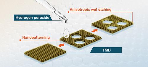
Here we will discuss our novel anisotropic wet-etching method that allows scalable fabrication of TMD metamaterials with atomic precision, combined with traditional nanolithography techniques.[1] We show that TMDs can be etched along certain crystallographic axes, such that the obtained edges are atomically sharp and exclusively zigzag-terminated. This allows us to fabricate interesting hexagonal nanostructures of predefined order and complexity, including a few nanometer thin nanoribbons and nanojunctions.
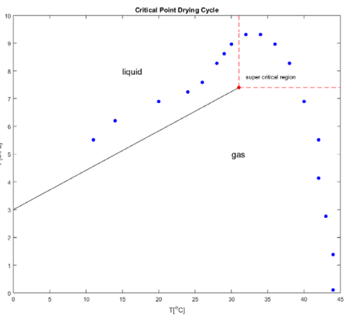
In this report I monitor a full successful cycle of critical point drying (CPD) run for drying MEMS sensors after wet release using KOH etching. The pressure and temperature of the CPD tool (Tousimis) is monitored during the process and plotted in a P-T diagram with \mathrm{CO_2} critical point. A few notes for higher yield in the drying process are mentioned in this report as well.
Results per page


