Bulk and Sleeve Electron Beam Lithography for Silicon Nitride Photonic Crystals

Abstract
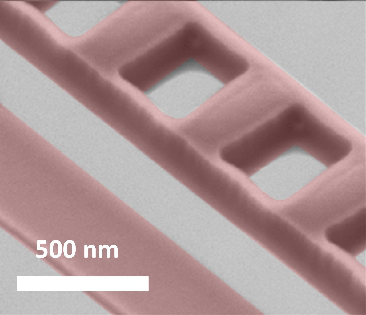
This is a method to improve the quality of lithography - in particular electron beam lithography (EBL). During an EBL exposure the electrons undergo different scattering processes. One scattering process that plays an important role is the back scattering of the electrons from the substrate or different stacks of thin film present in the exposure stack. As a result the actual dose that the resist sees is quite different that the original exposure dose. This difference can be fixed by means of proximity effect correction algorithms (PEC). In addition, the correction level that can be achieve via the PEC methods is limited to the absolute value of the dose and the back scattered electrons. As a result when the resolution is down to the limit of the resist, one might consider reducing the overall backscattered electron dosage by limiting the exposed area around the structure. Here we develop a process for making photonic crystals with high resolution EBL in silicon nitride.

Share

Authors
-
 EPFL - LPQM


Citations

 Waiting for citation...

Statistics


Comments (0)
Log in to comment & reply