We describe a fabrication process for electron beam lithography (EBL) and the following pattern transfer steps on transmission electron microscope (TEM) grids. For demonstration purposes, we use commercial off-the-shelf TEM grids consisting of a thin suspended silicon nitride membrane on a silicon frame supporting substrate. For the pattern transfer, we demonstrate both an additive patterning technique with metal deposition and lift-off, and a subtractive patterning technique with reactive ion etching. This process could enable direct ...
Results (2)
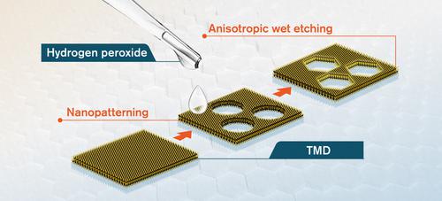
Here we will discuss our novel anisotropic wet-etching method that allows scalable fabrication of TMD metamaterials with atomic precision, combined with traditional nanolithography techniques.[1] We show that TMDs can be etched along certain crystallographic axes, such that the obtained edges are atomically sharp and exclusively zigzag-terminated. This allows us to fabricate interesting hexagonal nanostructures of predefined order and complexity, including a few nanometer thin nanoribbons and nanojunctions.
Results per page


