We describe a fabrication process for electron beam lithography (EBL) and the following pattern transfer steps on transmission electron microscope (TEM) grids. For demonstration purposes, we use commercial off-the-shelf TEM grids consisting of a thin suspended silicon nitride membrane on a silicon frame supporting substrate. For the pattern transfer, we demonstrate both an additive patterning technique with metal deposition and lift-off, and a subtractive patterning technique with reactive ion etching. This process could enable direct ...
Results (5)
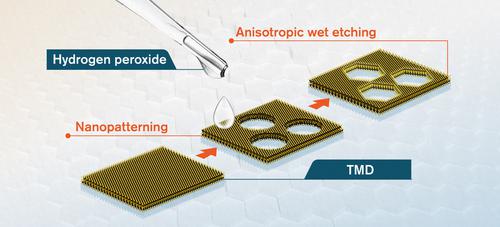
Here we will discuss our novel anisotropic wet-etching method that allows scalable fabrication of TMD metamaterials with atomic precision, combined with traditional nanolithography techniques.[1] We show that TMDs can be etched along certain crystallographic axes, such that the obtained edges are atomically sharp and exclusively zigzag-terminated. This allows us to fabricate interesting hexagonal nanostructures of predefined order and complexity, including a few nanometer thin nanoribbons and nanojunctions.
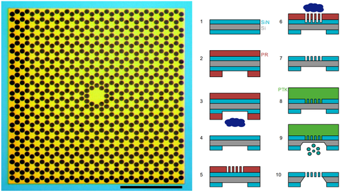
Thin silicon nitride nanomembranes are attracting growing attention following a novel fabrication method which consists in patterning them with a phononic crystal. In engineering the vibrational mode profile, the dominant mechanisms of loss, radiation loss and intrinsic material loss, are simultaneously addressed and mitigated. The fabrication method employed by the optomechanics group at the Laboratoire Kastler Brossel is here presented, only employing basic lithography techniques and wet etching processes.
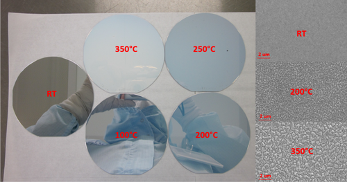
Here we present our study of the stress dependence in Al thin films on deposition conditions. We consider two types of Al 100-nm thick films: E-beam evaporated films and films obtained by magnetron sputtering. We investigate the Al film stress hysteresis in the environment with slowly increasing and decreasing temperature, i.e. during the gradual annealing. We consider the effect of deposition temperature on the film stress and grain size. We conclude that the annealing of ...
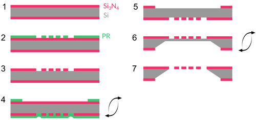
A fabrication method for large-area, high-stress LPCVD \mathrm{Si_3N_4} membranes is presented. These devices can be used as mechanical resonators with very low dissipation, exploiting dissipation dilution. A phononic crystal pattern allows to work with a high-order localized mode, shielded from acoustic radiation in the substrate. The procedure is amenable to most research clean rooms, requiring conventional lithography techniques and wet etching in KOH for device undercut.
Results per page


