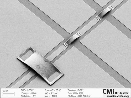
Here we discuss the wafer-scale fabrication process flow of aluminium airbridges for microwave (MW) interconnects on lithium niobate on Damascene silicon nitride (LNOD) photonic chips. We also discuss the subsequent chip release procedure that preserves the bridges allowing for safe release of these delicate structures.
Results (5)
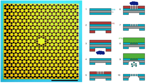
We describe a fabrication process for electron beam lithography (EBL) and the following pattern transfer steps on transmission electron microscope (TEM) grids. For demonstration purposes, we use commercial off-the-shelf TEM grids consisting of a thin suspended silicon nitride membrane on a silicon frame supporting substrate. For the pattern transfer, we demonstrate both an additive patterning technique with metal deposition and lift-off, and a subtractive patterning technique with reactive ion etching. This process could enable direct ...
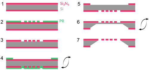
Thin silicon nitride nanomembranes are attracting growing attention following a novel fabrication method which consists in patterning them with a phononic crystal. In engineering the vibrational mode profile, the dominant mechanisms of loss, radiation loss and intrinsic material loss, are simultaneously addressed and mitigated. The fabrication method employed by the optomechanics group at the Laboratoire Kastler Brossel is here presented, only employing basic lithography techniques and wet etching processes.
A fabrication method for large-area, high-stress LPCVD \mathrm{Si_3N_4} membranes is presented. These devices can be used as mechanical resonators with very low dissipation, exploiting dissipation dilution. A phononic crystal pattern allows to work with a high-order localized mode, shielded from acoustic radiation in the substrate. The procedure is amenable to most research clean rooms, requiring conventional lithography techniques and wet etching in KOH for device undercut.
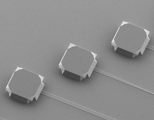
We describe the fabrication of high-stress Si_3N_4 nanobeam resonators with high aspect ratios exceeding lengths of 3.5mm. The lowest order out-of-plane modes of these nanobeams have quality factors of Q\geq 10^6 with fundamental mode frequencies lying in the range of 80-500kHz. The beams are fabricated from high-stress, 20-50nm-thick films of Si_3N_4 deposited via LPCVD on standard silicon wafers. The beams are patterned via electron beam lithography and deep reactive ion etching. The underlying silicon is ...
Results per page


