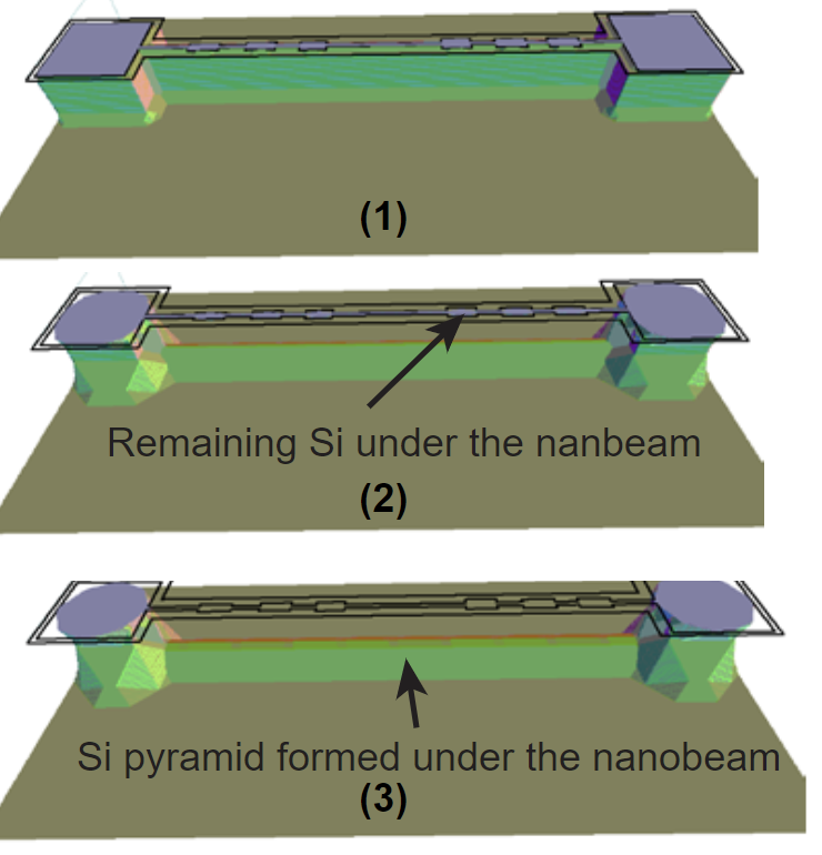
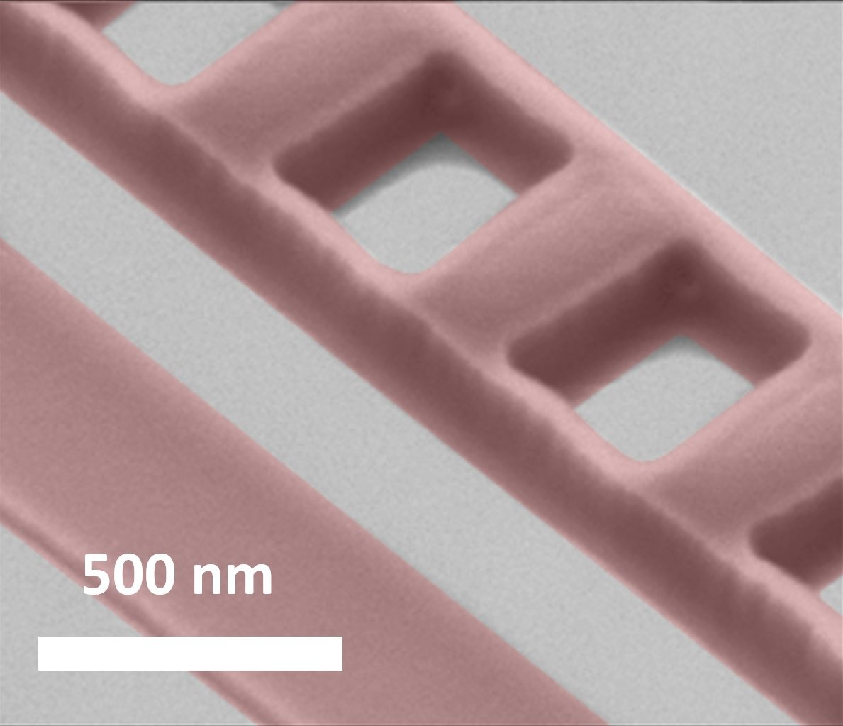
Search

Tooltip
Photo by Simon Escobar Steinvall, EPFL - LMSC

Results (5)


Monolithically integrated InGaAs microdisks on Si for nanophotonics

This work was presented at the Nanofabrication Photonics Online Meetup, 16-18 May 2021. Template-assisted selective epitaxy enables the local integration of group III-V semiconductors on Si with high material quality for nanophotonic applications. Here we demonstrate evidence of room temperature lasing at 1530 nm for a monolithically integrated InGaAs whispering gallery mode cavity on Si with a thickness of 300 nm and a diameter of 1.5 µm. These devices can potentially be scaled down further ...

Version
Version 1.0
Date
2 years, 10 months ago
Lab
IBM Research Zurich - Materials Integration and Nanoscale Devices
Comments
0
Viewed
1486
Downloads
578
Liked
3

Fabrication of patterned silicon nitride nanomembranes at the LKB

Thin silicon nitride nanomembranes are attracting growing attention following a novel fabrication method which consists in patterning them with a phononic crystal. In engineering the vibrational mode profile, the dominant mechanisms of loss, radiation loss and intrinsic material loss, are simultaneously addressed and mitigated. The fabrication method employed by the optomechanics group at the Laboratoire Kastler Brossel is here presented, only employing basic lithography techniques and wet etching processes.

Version
Version 1.1
Date
3 years, 6 months ago
Lab
Sorbonne - Kastler-Brossel
Comments
0
Viewed
3027
Downloads
1104
Liked
3

Dependence of stress in thin Al films on deposition and post-deposition temperature conditions

Here we present our study of the stress dependence in Al thin films on deposition conditions. We consider two types of Al 100-nm thick films: E-beam evaporated films and films obtained by magnetron sputtering. We investigate the Al film stress hysteresis in the environment with slowly increasing and decreasing temperature, i.e. during the gradual annealing. We consider the effect of deposition temperature on the film stress and grain size. We conclude that the annealing of ...

Version
Version 1.0
Date
3 years, 9 months ago
Lab
EPFL - LPQM
Comments
0
Viewed
1973
Downloads
776
Liked
1

Bulk and Sleeve Electron Beam Lithography for Silicon Nitride Photonic Crystals

This is a method to improve the quality of lithography - in particular electron beam lithography (EBL). During an EBL exposure the electrons undergo different scattering processes. One scattering process that plays an important role is the back scattering of the electrons from the substrate or different stacks of thin film present in the exposure stack. As a result the actual dose that the resist sees is quite different that the original exposure dose. This ...

Version
Version 1.0
Date
3 years, 10 months ago
Lab
EPFL - LPQM
Comments
0
Viewed
2179
Downloads
1115
Liked
1