Search

Tooltip
Photo by Julien Dorsaz, EPFL - CMi

Results (5)


Fabrication of aluminium airbridges for microwave interconnects on lithium niobate on Damascene silicon nitride photonic chips

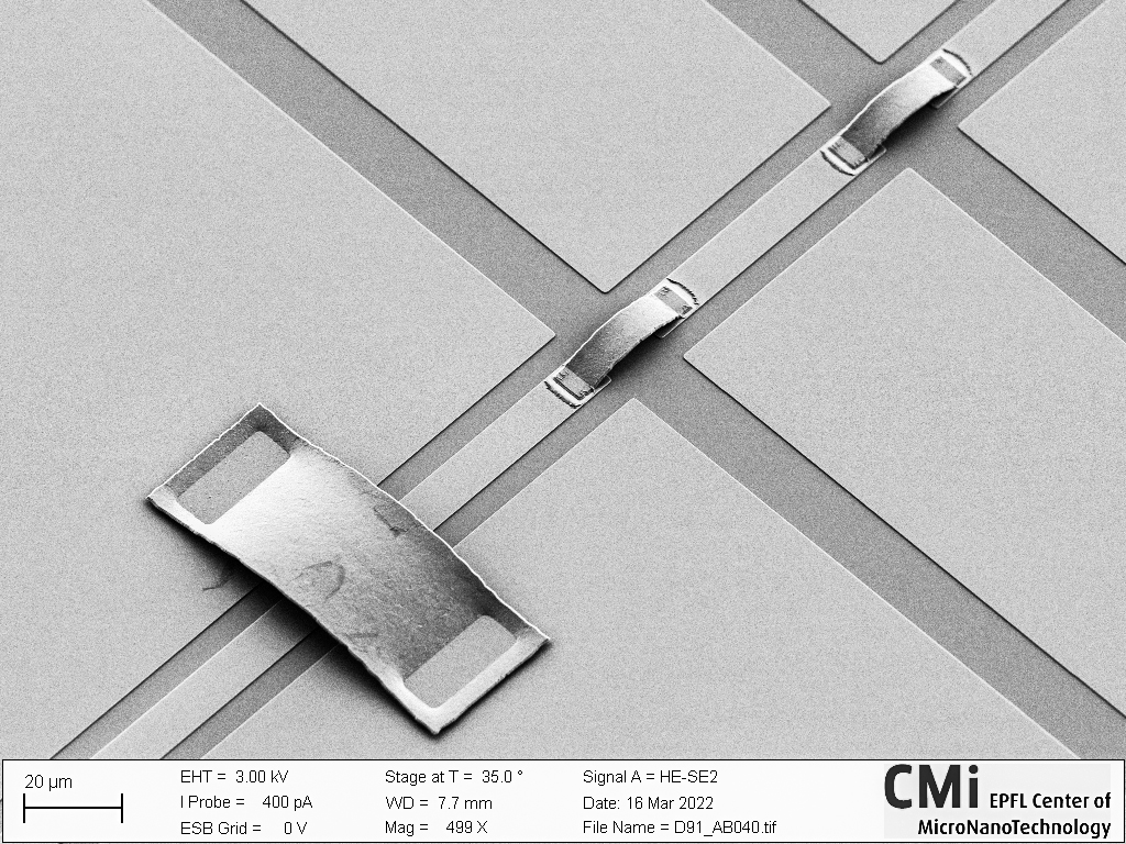
Here we discuss the wafer-scale fabrication process flow of aluminium airbridges for microwave (MW) interconnects on lithium niobate on Damascene silicon nitride (LNOD) photonic chips. We also discuss the subsequent chip release procedure that preserves the bridges allowing for safe release of these delicate structures.

Version
Version 1.1
Date
2 years, 7 months ago
Lab
EPFL - LPQM
Comments
0
Viewed
2281
Downloads
796
Liked
1

Electron beam lithography and pattern transfer on membrane grids for transmission electron microscopy

We describe a fabrication process for electron beam lithography (EBL) and the following pattern transfer steps on transmission electron microscope (TEM) grids. For demonstration purposes, we use commercial off-the-shelf TEM grids consisting of a thin suspended silicon nitride membrane on a silicon frame supporting substrate. For the pattern transfer, we demonstrate both an additive patterning technique with metal deposition and lift-off, and a subtractive patterning technique with reactive ion etching. This process could enable direct ...

Version
Version 1.1
Date
3 years, 8 months ago
Lab
EPFL - LPQM
Comments
0
Viewed
2770
Downloads
885
Liked
3


Monolithically integrated InGaAs microdisks on Si for nanophotonics

This work was presented at the Nanofabrication Photonics Online Meetup, 16-18 May 2021. Template-assisted selective epitaxy enables the local integration of group III-V semiconductors on Si with high material quality for nanophotonic applications. Here we demonstrate evidence of room temperature lasing at 1530 nm for a monolithically integrated InGaAs whispering gallery mode cavity on Si with a thickness of 300 nm and a diameter of 1.5 µm. These devices can potentially be scaled down further ...

Version
Version 1.0
Date
3 years, 11 months ago
Lab
IBM Research Zurich - Materials Integration and Nanoscale Devices
Comments
0
Viewed
1861
Downloads
765
Liked
3

Effect of LPCVD Si3N4\mathrm{Si_3N_4} deposition on Al2O3\mathrm{Al_2O_3} etch-stop films

Alumina (Al2O3\mathrm{Al_2O_3}) films are widely used in photonics and superconducting circuits as an etch stop or passivation layer. In silicon nitride (Si3N4\mathrm{Si_3N_4}) fabrication, a widely used etching recipe is dry etching using a mixture of SF6/CHF3\mathrm{SF_6/CHF_3} gasses. In case of multi-stacked materials, one might be interested to etch the Si3N4\mathrm{Si_3N_4} layer with an stop layer to protect the rest of the stack from the etching step. Al2O3\mathrm{Al_2O_3} is a great etch stop layer for Si3N4\mathrm{Si_3N_4} ...

Version
Version 1.0
Date
4 years, 11 months ago
Lab
EPFL - LPQM
Comments
0
Viewed
1747
Downloads
828
Liked
1