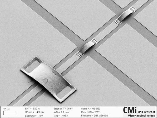
Here we discuss the wafer-scale fabrication process flow of aluminium airbridges for microwave (MW) interconnects on lithium niobate on Damascene silicon nitride (LNOD) photonic chips. We also discuss the subsequent chip release procedure that preserves the bridges allowing for safe release of these delicate structures.
Results (5)
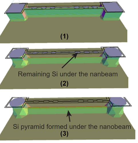
Here I explain the KOH simulator software (ACES) from University of Chicago [1] for a chain process of DRIE followed by KOH undercut. This software is very simple yet power to understand how Si etching works and design the mask to optimize the etch speed and crystal planes [2].
We describe a fabrication process for electron beam lithography (EBL) and the following pattern transfer steps on transmission electron microscope (TEM) grids. For demonstration purposes, we use commercial off-the-shelf TEM grids consisting of a thin suspended silicon nitride membrane on a silicon frame supporting substrate. For the pattern transfer, we demonstrate both an additive patterning technique with metal deposition and lift-off, and a subtractive patterning technique with reactive ion etching. This process could enable direct ...
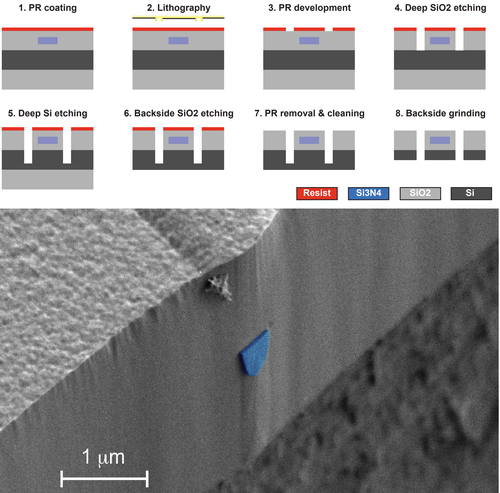
This short article describes a method to separate a wafer into photonic chips or dice, using dry etching and backside grinding. This method enables smooth chip facets that are advantageous for edge coupling with fibers or other chips.
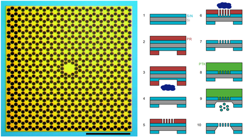
Thin silicon nitride nanomembranes are attracting growing attention following a novel fabrication method which consists in patterning them with a phononic crystal. In engineering the vibrational mode profile, the dominant mechanisms of loss, radiation loss and intrinsic material loss, are simultaneously addressed and mitigated. The fabrication method employed by the optomechanics group at the Laboratoire Kastler Brossel is here presented, only employing basic lithography techniques and wet etching processes.
Results per page


