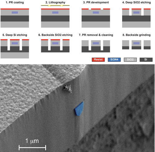
This short article describes a method to separate a wafer into photonic chips or dice, using dry etching and backside grinding. This method enables smooth chip facets that are advantageous for edge coupling with fibers or other chips.
Results (5)
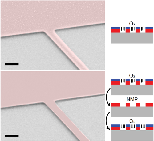
Resist removal is an essential step for multi-layer lithography processes where a clean and contamination-free surface is essential to avoid shadow etching patterns from resist leftovers. We show that a short \mathrm{O_2} plasma exposure followed by a full NMP solution cycle removes the resist fully and leaves the surface contamination free.
A few important points in data conversion and mask processing of multilayered Ebeam lithography is discussed. The conversion is done using Layout Beamer software at EPFL CMi cleanroom.
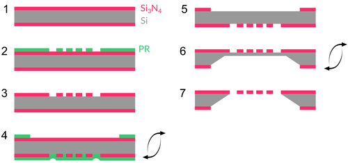
A fabrication method for large-area, high-stress LPCVD \mathrm{Si_3N_4} membranes is presented. These devices can be used as mechanical resonators with very low dissipation, exploiting dissipation dilution. A phononic crystal pattern allows to work with a high-order localized mode, shielded from acoustic radiation in the substrate. The procedure is amenable to most research clean rooms, requiring conventional lithography techniques and wet etching in KOH for device undercut.
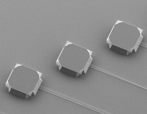
We describe the fabrication of high-stress Si_3N_4 nanobeam resonators with high aspect ratios exceeding lengths of 3.5mm. The lowest order out-of-plane modes of these nanobeams have quality factors of Q\geq 10^6 with fundamental mode frequencies lying in the range of 80-500kHz. The beams are fabricated from high-stress, 20-50nm-thick films of Si_3N_4 deposited via LPCVD on standard silicon wafers. The beams are patterned via electron beam lithography and deep reactive ion etching. The underlying silicon is ...
Results per page


