Search

Tooltip
Photo by Simon Escobar Steinvall, EPFL - LMSC

Results (5)


On the fabrication of high-surface-area and high-aspect-ratio gold nanostructures

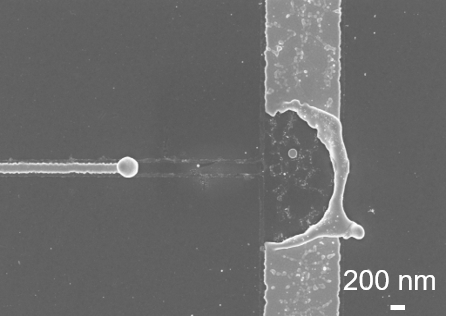
We highlight some stability issues in high-surface-area and high-aspect ratio gold nanostructures fabricated using inorganic adhesion layers on silica substrates. We ascribe these problems to capillary and surface effects and show the use of organic silane self-assembled monolayers to improve the long-term stability of such structures.

Version
Version 1.1
Date
2 years, 4 months ago
Lab
EPFL - NAM
Comments
0
Viewed
1458
Downloads
536
Liked
2

Electron beam lithography and pattern transfer on membrane grids for transmission electron microscopy

We describe a fabrication process for electron beam lithography (EBL) and the following pattern transfer steps on transmission electron microscope (TEM) grids. For demonstration purposes, we use commercial off-the-shelf TEM grids consisting of a thin suspended silicon nitride membrane on a silicon frame supporting substrate. For the pattern transfer, we demonstrate both an additive patterning technique with metal deposition and lift-off, and a subtractive patterning technique with reactive ion etching. This process could enable direct ...

Version
Version 1.1
Date
2 years, 6 months ago
Lab
EPFL - LPQM
Comments
0
Viewed
1714
Downloads
539
Liked
3


Monolithically integrated InGaAs microdisks on Si for nanophotonics

This work was presented at the Nanofabrication Photonics Online Meetup, 16-18 May 2021. Template-assisted selective epitaxy enables the local integration of group III-V semiconductors on Si with high material quality for nanophotonic applications. Here we demonstrate evidence of room temperature lasing at 1530 nm for a monolithically integrated InGaAs whispering gallery mode cavity on Si with a thickness of 300 nm and a diameter of 1.5 µm. These devices can potentially be scaled down further ...

Version
Version 1.0
Date
2 years, 10 months ago
Lab
IBM Research Zurich - Materials Integration and Nanoscale Devices
Comments
0
Viewed
1486
Downloads
578
Liked
3

Transition metal dichalcogenide metamaterials with atomic precision

Here we will discuss our novel anisotropic wet-etching method that allows scalable fabrication of TMD metamaterials with atomic precision, combined with traditional nanolithography techniques.[1] We show that TMDs can be etched along certain crystallographic axes, such that the obtained edges are atomically sharp and exclusively zigzag-terminated. This allows us to fabricate interesting hexagonal nanostructures of predefined order and complexity, including a few nanometer thin nanoribbons and nanojunctions.

Version
Version 1.0
Date
2 years, 11 months ago
Lab
DTU - Quantum Light Source
Comments
0
Viewed
1431
Downloads
596
Liked
3