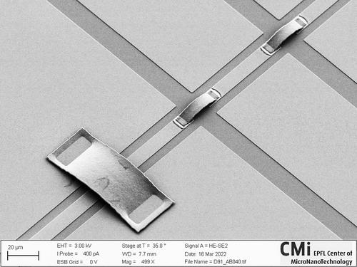
Here we discuss the wafer-scale fabrication process flow of aluminium airbridges for microwave (MW) interconnects on lithium niobate on Damascene silicon nitride (LNOD) photonic chips. We also discuss the subsequent chip release procedure that preserves the bridges allowing for safe release of these delicate structures.
Results (5)
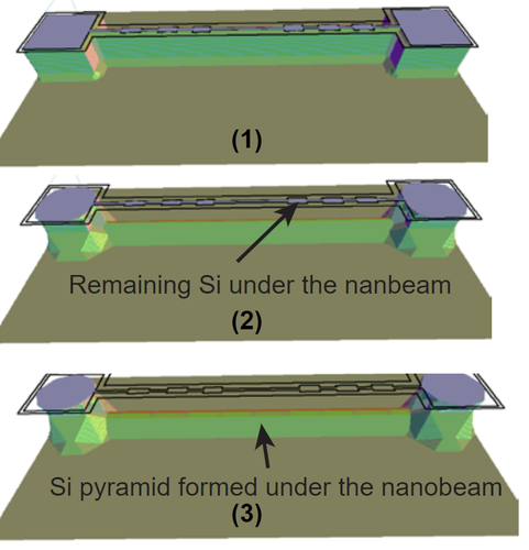
Here I explain the KOH simulator software (ACES) from University of Chicago [1] for a chain process of DRIE followed by KOH undercut. This software is very simple yet power to understand how Si etching works and design the mask to optimize the etch speed and crystal planes [2].
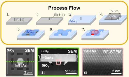
This work was presented at the Nanofabrication Photonics Online Meetup, 16-18 May 2021. Template-assisted selective epitaxy enables the local integration of group III-V semiconductors on Si with high material quality for nanophotonic applications. Here we demonstrate evidence of room temperature lasing at 1530 nm for a monolithically integrated InGaAs whispering gallery mode cavity on Si with a thickness of 300 nm and a diameter of 1.5 µm. These devices can potentially be scaled down further ...
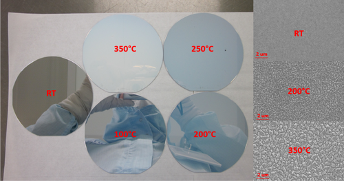
Here we present our study of the stress dependence in Al thin films on deposition conditions. We consider two types of Al 100-nm thick films: E-beam evaporated films and films obtained by magnetron sputtering. We investigate the Al film stress hysteresis in the environment with slowly increasing and decreasing temperature, i.e. during the gradual annealing. We consider the effect of deposition temperature on the film stress and grain size. We conclude that the annealing of ...
A few important points in data conversion and mask processing of multilayered Ebeam lithography is discussed. The conversion is done using Layout Beamer software at EPFL CMi cleanroom.
Results per page


