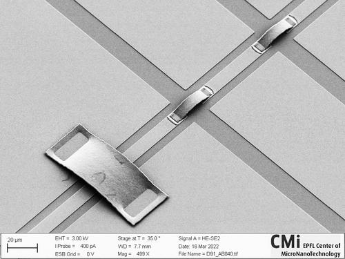
Here we discuss the wafer-scale fabrication process flow of aluminium airbridges for microwave (MW) interconnects on lithium niobate on Damascene silicon nitride (LNOD) photonic chips. We also discuss the subsequent chip release procedure that preserves the bridges allowing for safe release of these delicate structures.
Results (5)
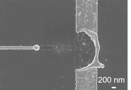
We highlight some stability issues in high-surface-area and high-aspect ratio gold nanostructures fabricated using inorganic adhesion layers on silica substrates. We ascribe these problems to capillary and surface effects and show the use of organic silane self-assembled monolayers to improve the long-term stability of such structures.
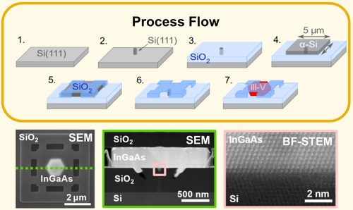
This work was presented at the Nanofabrication Photonics Online Meetup, 16-18 May 2021. Template-assisted selective epitaxy enables the local integration of group III-V semiconductors on Si with high material quality for nanophotonic applications. Here we demonstrate evidence of room temperature lasing at 1530 nm for a monolithically integrated InGaAs whispering gallery mode cavity on Si with a thickness of 300 nm and a diameter of 1.5 µm. These devices can potentially be scaled down further ...
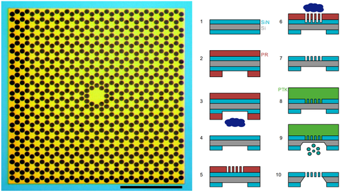
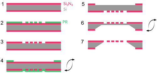
Thin silicon nitride nanomembranes are attracting growing attention following a novel fabrication method which consists in patterning them with a phononic crystal. In engineering the vibrational mode profile, the dominant mechanisms of loss, radiation loss and intrinsic material loss, are simultaneously addressed and mitigated. The fabrication method employed by the optomechanics group at the Laboratoire Kastler Brossel is here presented, only employing basic lithography techniques and wet etching processes.
A fabrication method for large-area, high-stress LPCVD \mathrm{Si_3N_4} membranes is presented. These devices can be used as mechanical resonators with very low dissipation, exploiting dissipation dilution. A phononic crystal pattern allows to work with a high-order localized mode, shielded from acoustic radiation in the substrate. The procedure is amenable to most research clean rooms, requiring conventional lithography techniques and wet etching in KOH for device undercut.
Results per page


